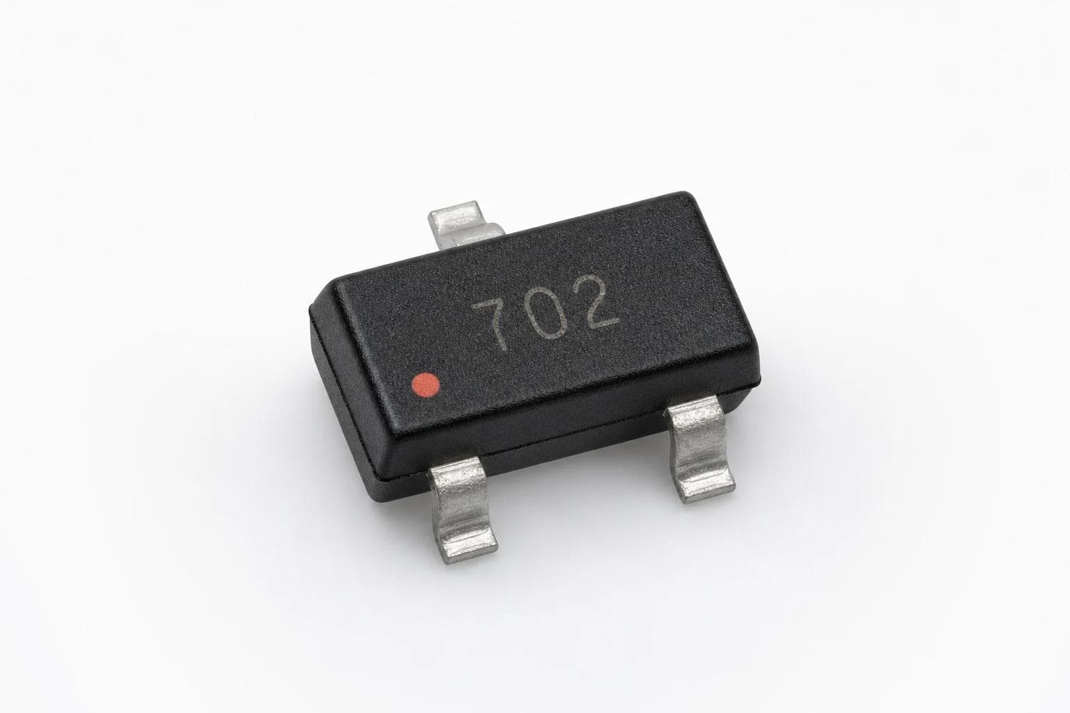
Logic-level switching is not defined by one headline voltage or current rating. A reliable selection starts with the actual gate voltage, load current, switching frequency, thermal path, and package constraints of the circuit.
1. Define the operating point
Translate the application into a small set of electrical conditions before comparing part numbers. Include steady-state load current, peak current, drain voltage, controller output voltage, ambient temperature, duty cycle, and required switching speed.
- Use the maximum drain-source voltage with adequate transient margin.
- Evaluate current at the real thermal condition rather than the absolute maximum headline rating.
- Check the gate drive at both nominal and minimum controller supply voltage.
2. Compare the parameters that change circuit behavior
| Parameter | Why it matters | Design question |
|---|---|---|
| VDS rating | Voltage withstand and transient margin | What is the highest repetitive and surge voltage? |
| RDS(on) | Conduction loss and voltage drop | Is it specified at the available VGS? |
| Qg / capacitance | Driver load and switching loss | Can the controller charge the gate fast enough? |
| Package thermal path | Junction temperature | Can the board remove the expected heat? |
| Threshold voltage | Beginning of conduction only | Is it being mistaken for a full-on voltage? |
Threshold voltage is not a substitute for an RDS(on) specification at the intended gate drive.
3. Treat the package as part of the electrical design
Small packages reduce board area but also concentrate thermal resistance and parasitic effects. Copper area, trace width, switching edge rate, and nearby heat sources can shift the practical current capability well below an absolute maximum rating.
Related product2N7002 SOT-23Use the 2N7002 product page as an example of how gate drive, current, package, and application context should be reviewed together.4. Validate the complete operating envelope
Finish selection by checking startup, fault, and elevated-temperature conditions. A short bench test should confirm gate waveform, switching transitions, device temperature, and voltage overshoot in the intended PCB layout.